| |
Lab 3: Datapath design
Due: Oct 22, 11:59pm. Submit on Canvas.
Weight: 15%
Goal.
The goal of this lab is to combine the blocks that were implemented in Lab 2 with a few other circuits and assemble a datapath.
For each computational block described below, you have to do the following:
- Write down production rules for the block, that describes the pull-up and pull-down networks to be used. Note that you can decide to use multiple stages of logic, use additional inverters, etc. as you see fit.
- Convert the production rules into the transistor-level implementation.
- Layout the transistor level implementation using magic
- Simulate your circuit using irsim to verify its functionality
Please read all parts of the lab before starting.
| Part 1: More datapath blocks |
For this part you will need to implement two circuits:
- An 8-bit register block, using the safe design discussed in class. The modification you should make is to design a register with two output ports (you can simply replicate the part of the register that provides the read control), called port0 and port1.
- An 8-bit latch, used to control the movement of data from its input to its output. Draw the latch without a staticizer on the output.
Use arrayable layout for both blocks.
Also, you should pitch-match the two new circuit blocks and the three computation blocks that were designed in lab 2. When you are done with this process, all the blocks should look like columns with almost identical heights.
Pitch matching: the idea here is that when you use the :array
command to array the one-bit layout, the pitch used for each one-bit
block that is arrayed (the combinational logic ones from the previous lab as
well as the two additional blocks above) should be identical.
| Part 2: Datapath assembly |
For this part you will assemble all your circuits into a single datapath.
-
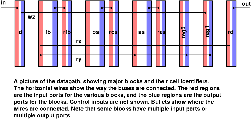
The datapath contains all the layout from lab2 and lab3. All the layout MUST BE pitch matched, otherwise wiring it up will be difficult. The layout should look like a sequence of vertical columns, with each column corresponding to a major 8-bit block. The order of the columns must be (from left to right, with cell identifier in parentheses): latch (ld); fblock (
fb); latch (rfb); oneshift (os); latch (ros); addsub (as); latch (ras); reg (reg0); reg (reg1); latch (rd).
-
Each of the latches will have independent control
-
The output of each combinational block must be connected to the input of the load block adjacent to it. That is, the data output of
fb, os, and as must be connected to the data input of rfb, ros, and ras respectively. This effectively adds a tristate buffer on the output of each combinational logic block.
-
Finally, wire up the inputs and outputs using three buses.
-
Each bit of the "a" input to each combinational block must be wired together using a single, horizontal strip of metal per bit (this is bus
rx in the picture below). This bus is also connected to the input of the rd (read) block, and output port 0 of registers reg0 and reg1.
-
Each bit of the "b" input to each combinational block must be wired together using a single, horizontal strip of metal per bit (this is bus
ry in the picture below). This bus is also connected to output port 1 of registers
reg0 and reg1.
-
Each bit of the output of each latch block (
rfb, ros, ras and ld) must be wired together using a single, horizontal strip of metal per bit (this is bus wz). This bus is also connected to the input port of registers reg0 and reg1.
-
Each bit of the bus
wz should have a staticizer on it. This
should also be arrayed.
-
Each bit of the output of the
rd block should also have a staticizer on it.
-
When you are done with the layout, you should have
- Top level input and outputs for data (the input to the "ld" block, and output of the "rd" block);
- Control signals for all the latches and registers, used to control the flow of data through the logic;
- Control signals for all the datapath blocks (addsub, fblock, shift).
A cartoon view of the layout and wiring is shown below:
Label the latch controls, and the primary input (in0..7) and output (out0..7) at the top-level of your layout. Once you've done this, you should be able to use the datapath to:
- Initialize the value of the two registers
- Read the two registers and use the any of the three combinational logic blocks (by selecting the appropriate control signals) to manipulate the values, and save the result in a register.
- Read the output of the register
Make sure you have test cases to check that each combinational logic block operates correctly, and that you can use the datapath as described above.
For this lab, turn in a zip file that contains:
- Your layout
- reg.mag, latch.mag, the layout for the 8-bit register and 8-bit latch (for part 1)
- datapath.mag (for part 2)
Make sure all sub-cells are included in your zip file.
The .mag files listed above are the "top-level" magic files for your layout
- The three corresponding irsim scripts that contains what you used to verify the functionality of your design
-
A PDF that summarizes what you did for this lab. The document should contain three parts (one per computation block), and each part should have:
- A one-page summary that contains
- A picture of your layout (just the 8-bit version).
- The maximum delay through the logic per irsim
- The area of your layout (in lambda units)
- An additional page (or multiple pages if you need them) that provide
- The production rules you used for the new circuits
- The transistor-level implementation used
- A description of any optimizations you might have used in the transistor-level implementation.
|